SMT Assembly Process Guidelines
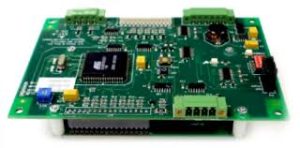
PCB (Printed Circuit Board) Surface Mount Technology (SMT) Assembly is a meticulous process that involves placing electronic components directly onto the surface of a PCB. To ensure high-quality, reliable electronic products, adhering to specific guidelines throughout the SMT assembly process is crucial. Here’s a comprehensive guide to the key steps and best practices involved in pcb smt assembly:
Choose a solder paste that is compatible with your PCB materials and components. Factors to consider include the type of flux, the size of the solder particles, and the paste’s viscosity. Design the stencil with precise openings that match the PCB pad layout. The stencil thickness should be optimized to ensure the correct volume of solder paste is applied. Common materials for stencils include stainless steel and nickel, which offer durability and precision.
Use an automated solder paste printer for consistent application. Ensure the PCB is securely positioned and aligned with the stencil. Verify the printing parameters, such as squeegee pressure, speed, and angle, to achieve uniform paste deposits. Program the pick-and-place machine with accurate component coordinates and placement sequences. Ensure that the machine’s vision system is calibrated to recognize component shapes and orientations correctly.
Handle components with care to avoid damage. Use appropriate nozzles and feeders to match the size and type of components. Check for component presence, orientation, and alignment before placement. Ensure high placement accuracy to prevent issues such as misalignment and tombstoning. Regularly inspect the machine’s performance and make adjustments as needed.
Develop a reflow profile that suits the solder paste and components used. The profile should include preheat, soak, reflow, and cooling stages. Each stage must be carefully controlled to prevent thermal shock and ensure proper solder joint formation. Use thermocouples to monitor the temperature at various points on the PCB. Ensure that the maximum temperature and ramp rates do not exceed the components’ specifications.

PCB SMT Assembly Process Guidelines
Consider using a nitrogen atmosphere in the reflow oven to reduce oxidation and improve solder joint quality. This is particularly useful for fine-pitch and complex assemblies. Implement AOI to check for defects such as solder bridges, insufficient solder, and component misalignment. AOI systems use high-resolution cameras and sophisticated algorithms to detect issues quickly and accurately.
Use X-ray inspection for hidden solder joints, especially for Ball Grid Arrays (BGAs) and other components with leads under the package. This helps identify voids, solder bridges, and insufficient solder. Complement automated inspections with manual inspections, especially for complex and high-value boards. Skilled operators can identify subtle defects that automated systems might miss.
Maintain detailed documentation of each step in the SMT assembly process. Include information on materials, equipment settings, inspection results, and any deviations from standard procedures. Establish a feedback loop between the assembly line and design and engineering teams. Use feedback to refine design guidelines, improve stencil and PCB layouts, and optimize process parameters.
Regularly train staff on the latest SMT assembly techniques and equipment. Encourage continuous learning and adaptation to new technologies and industry standards. By following these guidelines, manufacturers can enhance the quality, reliability, and efficiency of their PCB SMT assembly processes, ultimately delivering superior electronic products to the market.


