EMI/RFI shielding in custom pcb
Ensuring electromagnetic interference (EMI) and radio-frequency interference (RFI) shielding in custom printed circuit boards (PCBs) is critical for maintaining the reliability and performance of electronic devices, particularly in applications sensitive to electromagnetic disturbances. Various techniques and materials are employed to mitigate EMI/RFI and shield sensitive components and signals from external interference.
One approach to ensure EMI/RFI shielding in custom pcb is the use of shielding enclosures or covers. Shielding enclosures are metallic or conductive enclosures that surround the PCB or specific components, creating a barrier that blocks electromagnetic radiation from entering or exiting the device. These enclosures can be made from materials such as aluminum, copper, or steel, and may feature gaskets or seals to provide additional protection against EMI/RFI leakage.
In addition to shielding enclosures, conductive coatings or paints can be applied to the surface of custom PCBs to enhance EMI/RFI shielding. Conductive coatings are typically formulated with materials such as nickel, silver, or graphite, which create a conductive layer that reflects or absorbs electromagnetic radiation. These coatings can be applied to the entire PCB or specific areas where shielding is needed, providing an effective barrier against EMI/RFI interference.
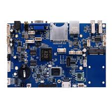
How do you ensure EMI/RFI shielding in custom pcb?
Furthermore, incorporating shielding elements directly into the PCB design can help mitigate EMI/RFI issues. Ground planes, for example, are conductive layers within the PCB that serve as reference planes for signal return paths and provide shielding against electromagnetic radiation. By properly designing and implementing ground planes in custom PCB layouts, designers can minimize EMI/RFI emissions and improve signal integrity.
Another effective technique for EMI/RFI shielding in custom PCBs is the use of shielding cans or cages. Shielding cans are metallic containers that encase individual components or sections of the PCB, providing localized shielding against electromagnetic interference. These cans are typically soldered or press-fit onto the PCB, creating a sealed enclosure that isolates sensitive components or signals from external interference sources.
Additionally, strategic placement of components and traces on the PCB can help minimize EMI/RFI emissions and susceptibility. By carefully arranging components and routing signal traces to minimize loop area and impedance mismatches, designers can reduce the likelihood of electromagnetic radiation and improve the overall EMI/RFI performance of the PCB.
Moreover, selecting appropriate materials for PCB substrates and laminates can contribute to EMI/RFI shielding. Certain materials, such as high-frequency laminates or conductive composites, offer enhanced electromagnetic compatibility (EMC) properties, reducing the transmission and reception of electromagnetic interference. By choosing materials with low dielectric loss and high electrical conductivity, designers can improve the EMI/RFI shielding effectiveness of custom PCBs.
Lastly, rigorous testing and validation procedures are essential for ensuring EMI/RFI shielding in custom PCBs. Conducting electromagnetic compatibility (EMC) testing, such as radiated emissions testing and susceptibility testing, helps identify potential sources of EMI/RFI and assess the effectiveness of shielding measures. By iteratively refining the PCB design based on testing results, designers can optimize EMI/RFI shielding and ensure compliance with regulatory standards and industry requirements.